PRESS RELEASES
Tomerdingen (Germany) - For immediate release - February 21, 2000
Foothill Instruments, LLC, a manufacturer of film thickness measurement systems and Boin GmbH, a metrology software manufacturer for the semiconductor industry, have signed an OEM agreement for the usage of Boin´s WAFERMAP software.
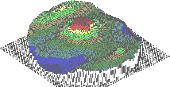
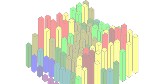
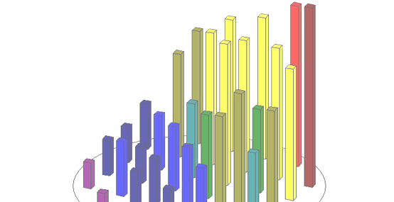
WAFERMAP, which runs under Windows 95 and NT4.0, is a scientific software application that allows the user to collect, edit, analyze and visualize measured physical parameters on semiconductor wafers. Data can be visualized by 1D, 2D or 3D plots. Several kinds of operations can be applied to the wafer maps or plots such as rotations, shifting of the grid in the X or Y direction, mirroring or reflecting of the data along the X and Y axis or averaging of radial zones. Global operations on the complete set of data such as adding, subtracting or multiplying by a constant can also be completed. WAFERMAP also allows the user to compare different sets of data by adding, subtracting or dividing complete wafer maps.
WAFERMAP has been integrated with the semi-automated KT-22 system to allow automatic mapping of the film's thickness across the wafer. The KT-22 allows thickness measurements of very thick films, ideal for advanced packaging, MEMS, magnetic recording, and other applications. The automatic stage handles substrates from 75 - 200 mm in diameter, including square substrates. It features non-contact measurements of 0.02 to greater than 90 µm of resist, for example.
Foothill Instruments states that "WAFERMAP was easily integrated with our software. This brought the KT-22 to market much faster and cheaper than if internally developed. Our customers have been delighted with the clarity of the data displayed with WAFERMAP."
A free Evaluation Copy of WAFERMAP can be downloaded at Download.
Contact:
Boin GmbH, Dr. Manuela Boin
E-Mail: info@boin-gmbh.com
Web: www.boin-gmbh.com
Tel: +49 (0) 7348-928233
Foothill Instruments, LLC
Tel: (888) 647-9280
Web: www.foothill-instruments.com