WAFERMAP
WAFERMAP – Semiconductor Wafer Metrology Data Analysis Software
WAFERMAP is an award-winning, vendor-independent semiconductor wafer metrology software designed to collect, edit, analyze and visualize measured physical parameters on 100, 150, 200 and 300 mm semiconductor wafers. The software enables process engineers, yield engineers and R&D teams to perform advanced wafer map analysis, metrology data visualization and process control optimization across multiple metrology platforms.
WAFERMAP imports measurement data from a wide range of semiconductor metrology tools, including ellipsometers, thin film thickness gauges, four-point probes, optical metrology systems and other wafer inspection equipment. As a flexible wafer data analysis tool, it consolidates data from different automatic and manual measurement systems into a unified visualization environment.
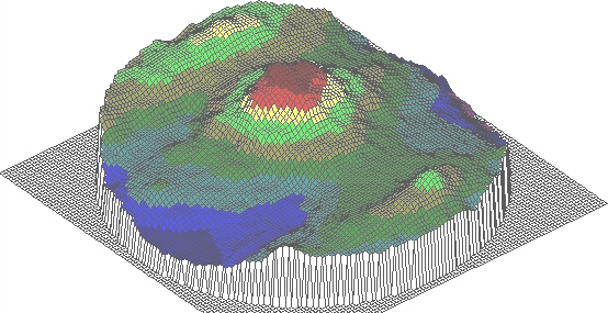
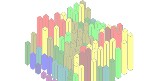
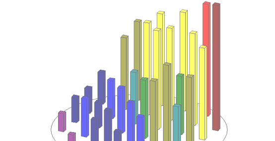
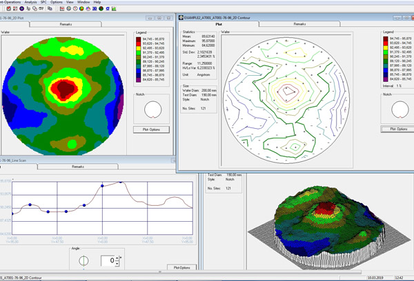
Imported data can be displayed as high-resolution line scans, contour plots, 2D wafer maps, 3D wafer surface visualizations or statistical histograms. Integrated statistical process control (SPC) capabilities support process drift detection, thin film uniformity analysis and yield optimization in semiconductor manufacturing.
Multiple wafer map operations are available, including rotation, grid shifting in X or Y direction, mirroring along X or Y axes and global mathematical operations such as addition, subtraction or first and second derivative analysis. Entire wafer maps can be compared by adding, subtracting or dividing data sets – ideal for tool-to-tool comparison and process qualification.
A configurable Sigma Filter eliminates measurement outliers beyond a user-defined tolerance range, improving data reliability and analysis accuracy. Typical applications include wafer map generation for manually operated metrology tools and standardized visualization across different automatic metrology equipment within the same fab environment.
WAFERMAP allows engineers to perform offline wafer metrology data analysis outside the clean room, reducing tool occupancy and supporting modern paperless semiconductor fabs. It is the ideal solution for flexible, cross-platform wafer map visualization and semiconductor process optimization.
Supported metrology data formats include, but are not limited to:
- 4 Dimensions
- AIT CMT 5000
- AMS SRD / MRD
- Bruker AXS
- CDE ResMap
- FILMetrics
- HRP-250
- KLA Tencor RS 100
- KLA Tencor F5 Ellipsometer
- Nanophotonics
- NanoSpec / AFT
- Napson WS300
- Nicolet
- Nova 2040
- OMS 3000
- OMT
- Plasmos
- Prometrix RS
- Prometrix UV-1250
- QC Solutions SCP 7000
- Rigaku 310Fab
- Rigaku MFM
- Rudolph
- Rudolph Metapulse
- Semitek
- Sentech SE-400
- Sentech SE-800
- SOPRA SE
- SpectraFilm F1
- Thermawave Optiprobe
- Thermaprobe
- TWIN

Editors’ Choice Best Product Award Presented to Boin GmbH
In developing a product that is truly making a difference in semiconductor manufacturing, Boin GmbH received the prestigious Editors’ Choice Best Product Award 1999, presented annually by Semiconductor International magazine, for its metrology software WAFERMAP. Semiconductor International announced 20 winners whose products are making a difference in semiconductor manufacturing.
You May Also Be Interested In
Explore Panelmap – a Powerful Software Solution for Rectangular Substrate Geometries.
Access Technical Application Notes – Advanced Wafer Map Analysis, Metrology Data Processing, and Engineering Use Cases.